Figure 1: A dual-height Unibus card
1.1 The history of the Unibus
1.2 The functionality of the Unibus
1.2.1 Physical functions
1.2.2 The ups and downs of a Unibus backplane
1.2.3 Addressing basics
1.3 Unibus card types
1.3.1 Module dimensions
1.3.2 Multi-module devices, modified system
units
1.3.3 Grant continuity, NPG grant
1.3.4 Miscellanous other equipment
1.4 Unibus hints and tips
1.4.1 Device arrangement
1.4.2 Working with Unibus systems
Note: These pages are for informational purposes, I cannot be held responsible for damages, loss of information/hardware or injuries. Take precautions, we're talking about sensitive equipment and electricity here! I gathered the information from handbooks, catalogs, UseNet postings and from my own experience, so I might be wrong here and there. Please mail me, if you find something that doesn't seem right!
1 Basics of the Digital Unibus
The Unibus was the main system component interconnect of the PDP-11 computer family. Designed around 1969/70, its main goal (and advantage at the same time) was that it provided means for all kind of system communication: there was only one bus in the PDP-11/20, which connected the CPU with memory AND all kind of peripherals. This was one of the first computers with a single bus (allthough later PDP-11 processors had other busses too, like a local memory-CPU interconnect or Massbus for peripheral interconnect). The bus itself had capabilities to use 18-bit addresses (with the memory management option installed in the CPU); only 16 were used in early implementations. Later 22-bit addressing was added with a special mapping mechanism.
Apart from PDP-11's, the Unibus was heavily used in early VAX computers too (VAX-11/780, 11/750, 11/730, 11/785, 8600), but in theses cases it wasn't the system bus anymore, it was used as a peripheral interconnect. The qbus, which was introduced in 1975 was based on the Unibus design.
1.2 The functionality of the Unibus
For those, who are new to Digital busses (or any busses for that matter): the Unibus is there to provide a way for the CPU (central processor unit, the heart of the computer) to communicate with the memory and different devices (peripheral controllers for example). Devices can use the Unibus to communicate with the CPU/memory or with another device. It's the processor's job to tell 'who' can use the bus for transferring data on it (this is called arbitration). Every device issues a request, when it needs to talk, the processor grants the right to do so according to multi-level priorities (which are determined by a priority list and/or by the physical distance of the device in question from the CPU) and the device becomes bus master. The bus master then selects the slave device, the one that receives the data from it. A device must be bus master to use the address lines; the address sent along those lines by the master is received by all bus devices that are capable of receiving slave grants. The one that recognizes its address becomes slave. Some devices are able to transfer to and from the memory without CPU intervention (DMA=Direct Memory Access; the CPU grants the access to the memory, and from then the requesting device is responsible for the further moves of data), mostly controllers that generate very much traffic; this speeds up things. The Unibus is an asynchronous interconnect, there's no central timing sequence, the functionality of the system depends on the proper use of request/grant/acknowledge signals (of course there are timeouts to prohibit bus hangs).
Logically, the Unibus is divided into the following parts: transmission lines (for request/grant signals: data and address, system status), arbitrator (which is in the CPU (PDP-11) or in the Unibus adapter (VAX with a different system bus)) and transmitters/receivers (which are on the devices (boards) itself). Mechanically, the Unibus consists of: the backplane (slots for the boards, interconnection between the connectors in the slots, plus wires for the electrical power), the card-edge connectors on the Unibus devices (these connecting fingers look just like the ones on qbus boards, which can be confusing sometimes - Digital used these card-edge connectors on many different type of busses, you should make sure that the card you're about to insert into a Unibus backplane is really a Unibus card!) and the signal termination on both ends. There's no "motherboard" on this bus as seen in the PC's for example: the bus is just a physical way to interconnect system components, and the CPU is just another device on it. The Unibus is a "daisy-chain"-type bus, devices are connected one after another. Basically, an empty slot between two Unibus devices means a break in the chain (it's not that easy, sometimes you can't tell if there's a break in the bus just by taking a look at it, as Unibus lines can be jumpered through slots via wire-wrapping on the back side).
1.2.2 The ups and downs of a Unibus backplane
As mentioned above, most Unibus-backplanes are wire-wrapped: on the back of the backplane you can see metallic pins for each pin of each slot: these can be connected with a piece of wire and a special tool (the wire-wrap tool/pistole). This of course means that a Unibus backplane can be rewired to something else. To make life more complicated, there are different types of slots in a Unibus backplane.
A Unibus backplane consists of one or more System Units. One system units usually provides place for 4 x 6 (4 rows, i.e. 4 x A-B-C-D-E-F) or 9 x 6 (9 rows, i.e. 9 x A-B-C-D-E-F) slots. The system units are connected to each other with jumper modules. The system units can be wired differently. There are two main sorts of "non-trivial" slots in a system unit:
The Unibus has memory mapped I/O addresses for each device in the system, which means that they communicate through special memory locations. The top 4096 word locations of the system memory are reserved for peripheral register addresses, each device on the Unibus has its device address in this range. The address is referred to as the Control and Status Register (CSR) address, and an interrupt vector. These values can be either fixed or floating addresses. Fixed means, that there are address locations in memory for the addresses of the particular option. E.g., there is a fixed address for the first device of the kind, for the second, the third, etc. Devices of the same type must use separate CSRs. A floating address is assigned a location within a range. Sometimes the first device of a particular kind is at a fixed address, and the next one is in the floating space.
As you will see, Unibus addresses (both the CSR and the vector) are displayed in octal values (the vectors are at the beginning of the address space, the CSR's are at the end). Physically, the addresses of a Unibus device can be set with jumpers or switches on the module. Modules with fixed addresses and vectors are usually shipped with settings for the first device of that particular kind. Vector addresses are often set by the opearting system upon boot. Also, in manuals and by some system software, these addresses are only referred to with six digits, i.e. 760215 is 177602150, or seven, i.e 7602150 is 177602150.
For example, the first MSCP (Digital's Mass Storage Control Protocol - a protocol used with disk drives from the mid-80's) disk controller CSR is at 772150, the other MSCP devices are in the floating CSR address space: 760334, 760340, 760344, etc...). The first TMSCP (which of course stands for Tape MSCP) has its CSR at 774500, the second TMSCP device has a floating CSR. On the other hand, the first Ethernet controller is at 774440, and the next at another fixed location, namely 774460. Finding the possible CSR and vector address values for a certain device is not trivial, but the manuals can help. Also of great help is the SYSGEN utility, which can be found on various Digital operating systems, e.g. RSX11, RSTS, VMS. This device addressing scheme is (nearly) the same with the qbus, so this utility can be used there too (it uses Unibus devices names anyhow).
Something about the terminology used here:
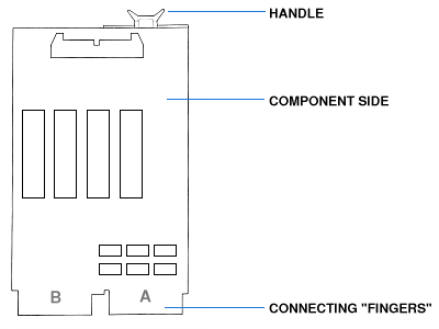
Dual-height card
Figure 1: A dual-height Unibus card
A dual card has two card-edge connecting "fingers". These two "fingers"
are enough to transmit and receive all Unibus signals and power, but most
Unibus boards are quad- or hex-height; dual cards are used e.g. for terminating/jumpering
the bus.
Quad-height card
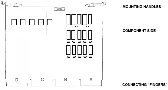
Figure 2: A quad-height Unibus card
The quad boards have four "fingers". A slot which accomodates a module like this is called SPC, Small Peripheral Controller slot. We'll see examples for this, one thing's for sure: there are different types of backplanes, one must pay attention when moving around cards between different systems!).
Hex-height card
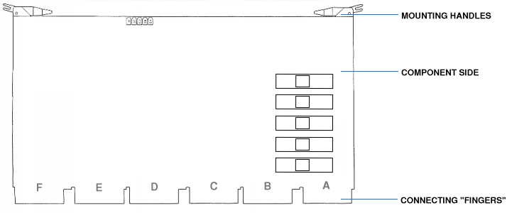
Figure 3: A hex-height Unibus module
A hex module has six "fingers". On the drawing above the fingers are labelled with letters A-F, this helps with the orientation when inserting a card into a backplane. As we'll see later, there are different kinds of Unibus slots.
Handles and identification
"Normal" Unibus cards (well... most of them) have small plastic handles on the end of the bord, and/or small metal "hooks" that are used to hold it in place and help at insertion or removal. There are small "bumps" with the module number engraved on the spine of the boards. A hex card has two "bumps" like this, one has got the module number (e.g. M7850) on it, the other the revision (e.g. "-YB"). The module number and sometimes even the name of the option (like "UDA50" or "KY11-AA") is etched onto the PCB surface (but there's no "general" place for it, you'll have to look after it if the module is densly populated).
1.3.2 Multi-module devices, modified system units
As mentioned earlier, some devices can occupy more than one Unibus boards (mostly 2 or 3). Sometimes these are connected with ribbon cables, sometimes some of the slots (like A and B) are used as a local interconnect between several cards (the benefits of wire-wrapping!).
There are devices, that have their own backplane, which looks like just a Unibus System Unit, but is wired differently. Don't insert a normal Unibus module into a backplane like that without inspecting it! A good example is the RH11 Massbus controller: its system unit's "input" and "output" (slots 9A-B and 1A-B) is Unibus, but the RH11 cards sit in modified slots.
1.3.3 Grant continuity jumper card, NPG jumper
A grant continuity card is used to jumper signals through an empty slot (its normal place is in slot C-D). There's another kind of jumpering, the NPG (non-processor grant), which is done by placing a wire-wrap jumper on the respecting two pins on the back of the backplane (CA1 and CB1). This must be installed if the SPC slot's empty or if the device in that slot is using DMA! You can find it out by looking at the top pin on both side of the C "finger": if they're connected to the logic, the module uses DMA, and the jumper must be removed. If these two pins are connected to each other, the module doesn't utilizes DMA, but it jumpers the NPG signals - no jumper needed. If the two pins are not connected to anything, you must insert the wire-wrap on the backside of the backplane. And vica versa: if you install a DMA device in an empty SPC slot, make sure that this jumper is removed! (sometimes this jumper is pre-installed and you must remove a wire or a 0-ohm resistor).
1.3.4 Miscellanous Unibus equipment
Unibus cable (or "Unibus jumper")
A jumper card (a set of two dual cards connected with ribbon cables) is used to connect two Unibus system units. There are rules how to do this, as the length of the Unibus is limited. The cards must be inserted into the "Unibus in" and "Unibus Out" slots (these are usually slot A-B in the first and last row of a system unit). Never insert a Unibus cable into a MUD (Modified Unibus Device) slot (a slot in which A and B carry non-Unibus signals (and sometimes current too), this can blow things away!
A "Unibus cable" (e.g. a BC11-A) is the same with longer cable between the two cards, this can be used to connect Unibus system units in two expansion boxes. It has 56 signal lines and 64 ground lines (to prevent noise intermission), maximal length is normally 25 feet (8.6 m).
Unibus terminators
The Unibus needs to be properly terminated in order to prohibit signal reflections. The terminator module needs to be inserted into a "Unibus out" slot, which is normally used to connect the bus chain to another system unit (don't insert it into a MUD slot!). The older M920 and M930 modules have a terminatation of 178 ohms to +5V and 383 ohms to GND, some newer cards (M9201) also have bootstrap/diagnostic PROMs on-board.
There are two main factors you should take notice of when arranging Unibus devices:
These are just things that pop to my mind...
Back to the top
On to "Unibus systems"
Full Table of Contents
Back to the main page
| Copyrights: Ákos Varga, 1999 | Last modified: |